- 您现在的位置:买卖IC网 > Sheet目录3881 > PIC18F8720T-E/PT (Microchip Technology)IC PIC MCU FLASH 64KX16 80TQFP
R01DS0060EJ0100 Rev.1.00
Page 148 of 168
Sep 13, 2011
RX630 Group
5. Electrical Characteristics
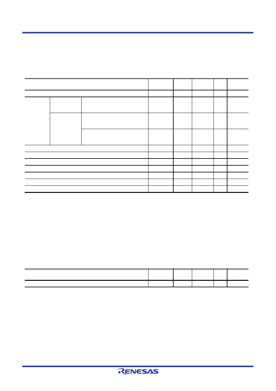
Note: When A/D conversion is done during access to the external bus, the accuracy may degrade.
In this case, repeat conversion several times and calculate by software the average of the converted values, excluding the
maximum and minimum values.
Note 1. The conversion time includes the sampling time and the comparison time. As the test conditions, the number of sampling states
is indicated.
Note 2. The value in parentheses indicates the sampling time.
Table 5.22
12-Bit A/D Conversion Characteristics
Conditions: VCC = AVCC0 = VCC_USB = 2.7 to 3.6 V, VREFH/VREFH0 = 2.7 V to AVCC0
VSS = AVSS0 = VREFL/VREFL0 = VSS_USB = 0 V
PCLK = 8 to 50 MHz
Ta = Topr
Item
Min.
Typ.
Max.
Unit
Test
Conditions
Resolution
12
Bit
Conversion
(Operation
at PCLK =
50 MHz)
AN0 to AN7
Permissible signal source impedance
(max.) = 1.0 k
1.0 (0.4)*2
—
s
Sampling
in 20
states
Other channels
Permissible signal source impedance
(max.) = 1.0 k
, AVCC
3.0 V
2.0 (1.4)*2
—
s
Sampling
in 70
states
Permissible signal source impedance
(max.) = 1.0 k
, AVCC
2.7 V
5.6 (5.0)*2
—
s
Sampling
in 250
states
Analog input capacitance
—
30
pF
Offset error
—
±2.0
±7.5
LSB
Full-scale error
—
±2.0
±7.5
LSB
Quantization error
—
±0.5
—
LSB
Absolute accuracy
—
±2.5
±8.0
LSB
DNL differential nonlinearity error
—
±2.0
±4.0
LSB
INL integral nonlinearity error
—
±2.0
±4.0
LSB
Table 5.23
A/D Internal Reference Voltage Characteristics
Conditions: VCC = AVCC0 = VCC_USB = 2.7 to 3.6 V, VREFH/VREFH0 = 2.7 V to AVCC0
VSS = AVSS0 = VREFL/VREFL0 = VSS_USB = 0 V
PCLK = 8 to 50 MHz
Ta = Topr
Item
Min.
Typ.
Max.
Unit
Test
Conditions
A/D Internal reference voltage
1.45
1.50
1.55
V
发布紧急采购,3分钟左右您将得到回复。
相关PDF资料
PIC18F4439T-E/ML
IC PIC MCU FLASH 6KX16 44QFN
XF2J-2824-11
CONN FPC 28POS 0.5MM SMT
PIC18F4439T-E/PT
IC PIC MCU FLASH 6KX16 44TQFP
PIC18F6585T-I/PT
IC PIC MCU FLASH 24KX16 64TQFP
PIC18LF8525T-I/PT
IC PIC MCU FLASH 24KX16 80TQFP
PIC18F6720T-E/PT
IC PIC MCU FLASH 64KX16 64TQFP
PIC18F4539T-E/PT
IC PIC MCU FLASH 12KX16 44TQFP
PIC16F685-I/P
IC PIC MCU FLASH 4KX14 20DIP
相关代理商/技术参数
PIC18F8720T-I/PT
功能描述:8位微控制器 -MCU 128KB 3840 RAM 68I/O RoHS:否 制造商:Silicon Labs 核心:8051 处理器系列:C8051F39x 数据总线宽度:8 bit 最大时钟频率:50 MHz 程序存储器大小:16 KB 数据 RAM 大小:1 KB 片上 ADC:Yes 工作电源电压:1.8 V to 3.6 V 工作温度范围:- 40 C to + 105 C 封装 / 箱体:QFN-20 安装风格:SMD/SMT
PIC18F8721-I/PT
功能描述:8位微控制器 -MCU 128kBF 4096RM 40MHz nonoWatt RoHS:否 制造商:Silicon Labs 核心:8051 处理器系列:C8051F39x 数据总线宽度:8 bit 最大时钟频率:50 MHz 程序存储器大小:16 KB 数据 RAM 大小:1 KB 片上 ADC:Yes 工作电源电压:1.8 V to 3.6 V 工作温度范围:- 40 C to + 105 C 封装 / 箱体:QFN-20 安装风格:SMD/SMT
PIC18F8721T-I/PT
功能描述:8位微控制器 -MCU 128kBF 4096RM 40MHz nonoWatt RoHS:否 制造商:Silicon Labs 核心:8051 处理器系列:C8051F39x 数据总线宽度:8 bit 最大时钟频率:50 MHz 程序存储器大小:16 KB 数据 RAM 大小:1 KB 片上 ADC:Yes 工作电源电压:1.8 V to 3.6 V 工作温度范围:- 40 C to + 105 C 封装 / 箱体:QFN-20 安装风格:SMD/SMT
PIC18F8722 DEVELOPMENT BOARD KIT
功能描述:DEVELOPMENT BOARD FOR PIC18F8722 RoHS:否 类别:编程器,开发系统 >> 通用嵌入式开发板和套件(MCU、DSP、FPGA、CPLD等) 系列:- 标准包装:1 系列:PICDEM™ 类型:MCU 适用于相关产品:PIC10F206,PIC16F690,PIC16F819 所含物品:板,线缆,元件,CD,PICkit 编程器 产品目录页面:659 (CN2011-ZH PDF)
PIC18F8722 DEVELOPMENT KIT
功能描述:EMBEDDED C DEVELOPMENT KIT RoHS:否 类别:编程器,开发系统 >> 通用嵌入式开发板和套件(MCU、DSP、FPGA、CPLD等) 系列:PIC® 产品培训模块:Blackfin® Processor Core Architecture Overview
Blackfin® Device Drivers
Blackfin® Optimizations for Performance and Power Consumption
Blackfin® System Services 特色产品:Blackfin? BF50x Series Processors 标准包装:1 系列:Blackfin® 类型:DSP 适用于相关产品:ADSP-BF548 所含物品:板,软件,4x4 键盘,光学拨轮,QVGA 触摸屏 LCD 和 40G 硬盘 配用:ADZS-BFBLUET-EZEXT-ND - EZ-EXTENDER DAUGHTERBOARDADZS-BFLLCD-EZEXT-ND - BOARD EXT LANDSCAP LCD INTERFACE 相关产品:ADSP-BF542BBCZ-4A-ND - IC DSP 16BIT 400MHZ 400CSBGAADSP-BF544MBBCZ-5M-ND - IC DSP 16BIT 533MHZ MDDR 400CBGAADSP-BF542MBBCZ-5M-ND - IC DSP 16BIT 533MHZ MDDR 400CBGAADSP-BF542KBCZ-6A-ND - IC DSP 16BIT 600MHZ 400CSBGAADSP-BF547MBBCZ-5M-ND - IC DSP 16BIT 533MHZ MDDR 400CBGAADSP-BF548BBCZ-5A-ND - IC DSP 16BIT 533MHZ 400CSBGAADSP-BF547BBCZ-5A-ND - IC DSP 16BIT 533MHZ 400CSBGAADSP-BF544BBCZ-5A-ND - IC DSP 16BIT 533MHZ 400CSBGAADSP-BF542BBCZ-5A-ND - IC DSP 16BIT 533MHZ 400CSBGA
PIC18F8722-E/PT
功能描述:8位微控制器 -MCU 128 KB FL 3936 RAM 25 MHz RoHS:否 制造商:Silicon Labs 核心:8051 处理器系列:C8051F39x 数据总线宽度:8 bit 最大时钟频率:50 MHz 程序存储器大小:16 KB 数据 RAM 大小:1 KB 片上 ADC:Yes 工作电源电压:1.8 V to 3.6 V 工作温度范围:- 40 C to + 105 C 封装 / 箱体:QFN-20 安装风格:SMD/SMT
PIC18F8722-I/PT
功能描述:8位微控制器 -MCU 128 KB FL 4K RAM 70 I/O RoHS:否 制造商:Silicon Labs 核心:8051 处理器系列:C8051F39x 数据总线宽度:8 bit 最大时钟频率:50 MHz 程序存储器大小:16 KB 数据 RAM 大小:1 KB 片上 ADC:Yes 工作电源电压:1.8 V to 3.6 V 工作温度范围:- 40 C to + 105 C 封装 / 箱体:QFN-20 安装风格:SMD/SMT
PIC18F8722T-E/PT
功能描述:8位微控制器 -MCU 128 KB FL 3936 RAM 25MHz RoHS:否 制造商:Silicon Labs 核心:8051 处理器系列:C8051F39x 数据总线宽度:8 bit 最大时钟频率:50 MHz 程序存储器大小:16 KB 数据 RAM 大小:1 KB 片上 ADC:Yes 工作电源电压:1.8 V to 3.6 V 工作温度范围:- 40 C to + 105 C 封装 / 箱体:QFN-20 安装风格:SMD/SMT